
Moat GOAT: EDA software
The duopoly of Cadence and Synopsys

From smartphones to electric vehicles, nearly every modern device runs on chips—intricate assemblies of complex circuits. While chip designers are making headlines thanks to AI, have you wondered what tools they use to design these circuits?
Let’s dive into the world of electronic design automation (EDA) software and the two giants at its helm: Cadence and Synopsys, two companies who delivered some of the highest total shareholder returns over the past decade.
How does a chip get designed?

Every chip starts as an idea. Engineers define its specifications based on customer needs, deciding whether it will be a CPU (like the Intel chip in your PC), GPU (Nvidia of course), ASIC (use case-specific chips), and selecting fabrication technology (eg. 5nm or 7nm nodes.)
Next comes architectural design, where engineers determine the chip’s building blocks—processor cores, memory, and interconnects—and map out data flow between them. Once finalized, they create a high-level circuit model using a hardware description language (HDL) like Verilog, essentially drafting a blueprint.

In circuit design, blueprint is translated into transistor-level circuits. Every detail—timing, power efficiency, and noise—must be optimized for reliability. EDA tools simulate and refine the design before moving to physical design, where the abstract logic is transformed into a silicon layout. Components are placed, wire routing is optimized, and checks ensure manufacturability.

Before manufacturing, engineers run timing analysis and power optimization. The design then undergoes verification, including simulations, hardware emulations, and formal verification to catch potential errors.
Once approved, the design moves to fabrication, where it is converted into photolithographic masks and sent to foundries for production.

After wafer fabrication, chips are tested and packaged. Final functional and reliability tests confirm they meet specifications before release.
Finally, the chip is deployed in real-world applications, powering everything from smartphones to data centers and autonomous vehicles. Engineers monitor its performance, gather feedback, and refine future iterations.
History of EDA software
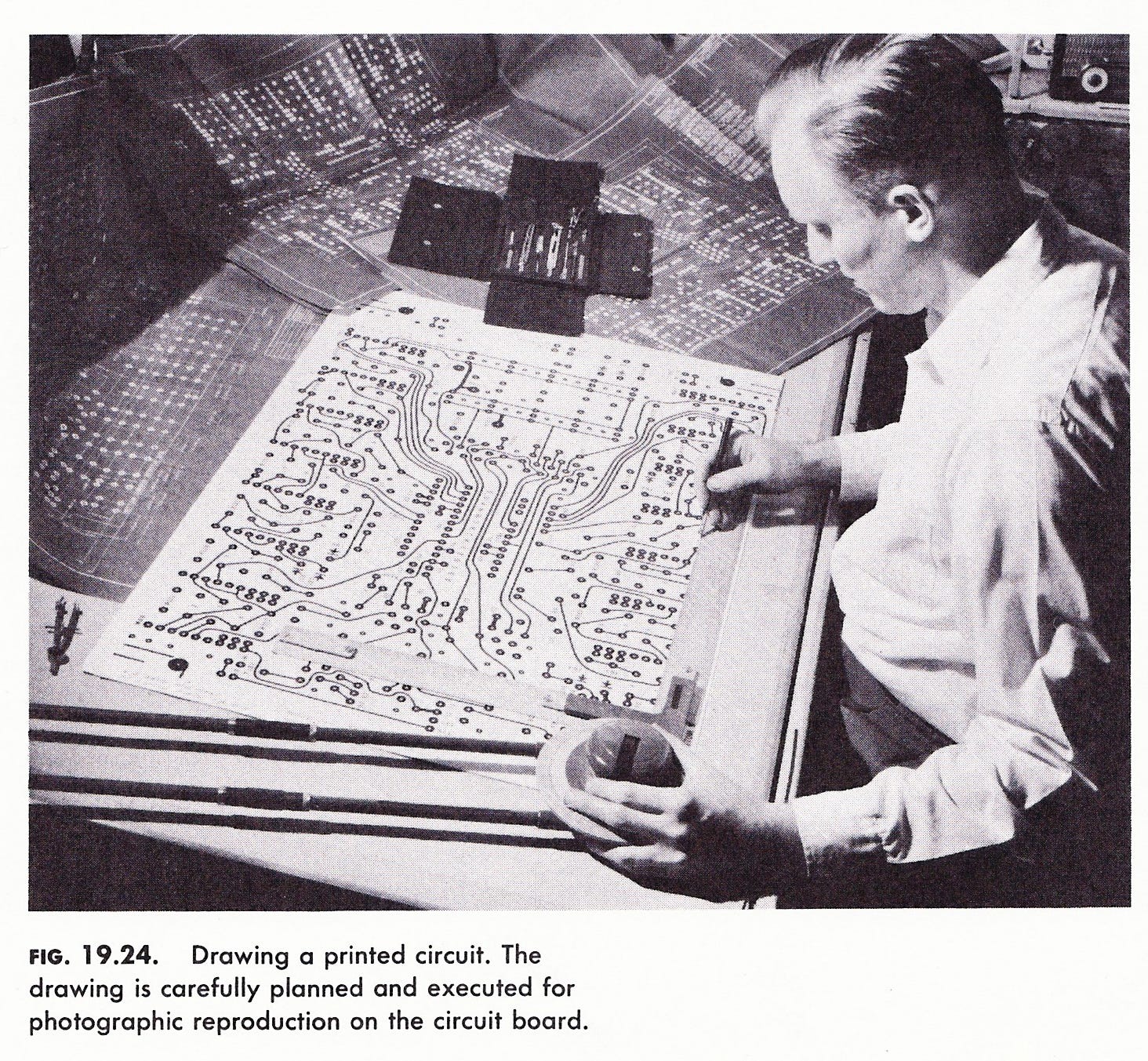
Before EDA software, circuits were designed entirely by hand, using drafting tools and paper. Engineers manually transferred these designs onto photomasks, making the process labor-intensive and error-prone.
In the 1970s, the first versions of EDA software emerged, developed large tech companies like IBM and Texas Instruments for in-house use. They had limited features, focusing on automating basic tasks.

As demand for more complex designs increased, a new generation of standalone EDA companies appeared. These companies created more comprehensive tools for semiconductor design. By the end of the 1970s, EDA software had become the industry standard for chip design.
By the 1980s, customers needed more sophisticated EDA tools to handle the growing complexity of chip designs, as number of transistors grew exponentially driven by Moore’s Law.
At the same time, the structure of semiconductor industry underwent a major shift. Until the late 1980s, most semiconductor firms were vertically integrated, handling both chip design and manufacturing in-house, often using proprietary design tools. The introduction of the fabless business model changed everything: companies could now design chips using third-party EDA software and outsource fabrication to dedicated foundries like TSMC, which was founded in 1987.
The availability of workstations and personal computers made it easier for companies to run EDA tools on their own systems without needing to purchase an integrated software-and-hardware device.
This shift opened the door for new EDA leaders.
Synopsys was founded in 1986 and introduced the first commercially successful logic synthesis tool, which allowed engineers to focus on high-level design while letting software handle the low-level translation into circuit layouts.
Cadence was formed in 1988 through the merger of SDA Systems and ECAD, pioneering a new generation of place-and-route tools that automated the physical layout of chips.

Throughout the 1990s, Synopsys and Cadence became dominant players, with Synopsys specializing in the front-end (logic synthesis) and Cadence leading in the back-end (physical layout and verification). Over time, Mentor Graphics (now Siemens EDA) emerged as another key player, completing the "Big Three" of EDA.
The EDA industry has consolidated due to:
The increasing complexity of chips favors tools sophisticated enough for leading-edge customers.
Synopsys and Cadence have expanded through acquisitions, offering features in a market that favors platform solutions.
New entrants have either been bought or struggle to grow because larger customers are happily served by the incumbents.
Today, every major semiconductor company—from Nvidia to AMD—relies on EDA software to design and simulate chips before they are manufactured by foundries like TSMC.
Over the last decade, Cadence and Synopsys have transitioned from license-based pricing to subscription-based pricing. Synopsys is reported to have a customer retention rate of ~95%. This, combine with consolidating market shares and industry growth, led to multiple expansion in addition to their revenue growth.
Semiconductor IP - An adjacent opportunity
Another monetization strategies for EDA software vendors is upselling semiconductor intellectual property (IP).

A chip consists of components that provide set functionalities. Instead of designing every component from scratch, chipmakers can purchase pre-verified IP blocks—such as Wi-Fi, USB device, or PCIe controllers—and integrate them into their designs. These IP blocks have been extensively tested across many customer applications, ensuring reliability and accelerating product development.
The semiconductor IP business is just like a media and software business that follows a "design once, sell infinitely" model, where IP owners earn royalties based on usage.
Why would customers pay for IPs instead of developing their own?
Proven IP shortens development cycles and provides a time-to-market advantage. Complex chip components takes year to develop.
Enhances reliability by minimizing the risk of design flaws and compatibility issues as the IPs are extensively tested by the IP holder and through usage in customers’ designs across many use cases.
Cost savings, as developing in-house IP requires heavy engineering resources.
Ecosystem compatibility: many foundries and design tools support seamless integration with validated IPs.
IP vendors offer technical support and customization, allowing companies to tailor IP to their specific needs.
The semiconductor IP market is dominated by a few major players, such as Arm, Synopsys, and Cadence. Similar to EDA market, IP market has very high barrier to entry due to:
deep technical expertise
high R&D costs
proven compatibility with customer products and industry standards
difficulty of earning trust from major customers (such as Apple and Nvidia) who use proven IP in mission-critical designs. For example, once a vendor like Arm achieves widespread adoption, its ecosystem, including software, compilers, and toolchains, becomes optimized for its architecture.
Patent and legal barriers: Startups risk infringing on existing patents, and legal challenges from established firms can be a significant deterrent to new entrants.
7 Powers
Under the 7 Powers framework, what makes the EDA and IP industry great?
Scale economics
R&D is very expensive for EDA and IP development, requiring engineers, testing cost and industry standard compliance costs. Cadence and Synopsys have a big dollar profit pool to reinvest into R&D.
By continuously improving their offerings, these companies strengthen their market dominance and make it even harder for smaller competitors to gain traction.
Switch Costs
Switching EDA tools or IP providers incurs big costs and risks.
Migrating designs from one platform to another can result in compatibility issues, requiring manual adjustments and additional verification steps. This creates both a productivity risk, as engineers spend time troubleshooting instead of innovating, and a defect risk, where unintended errors could affect chip performance.
For example, Synopsys IP is often pre-validated and optimized with its EDA tools, customers benefit from improved performance, power efficiency, and area optimization. Simplified licensing and procurement reduce overhead and costs, while customers may also gain early access to new IP releases and customization options, keeping their designs competitive.
In the era of AI war, lagging in speed-to-market and design errors mean losing in a new paradigm shift.

Cornered Resource
Cadence and Synopsys are the only games in town for EDA and IP, they have pricing power without needing big reinvestment (software and IP have similar “build once sell infinitely” dynamics.) - recipe for consistently high ROIC.
Each EDA tool contains millions of lines of code that have been refined over decades. Startups entering this space often spend more than five years just reaching feature parity. It’s not enough to match the incumbents—startups must offer better solutions to convince users to switch, a nearly impossible task since incumbents are also evolving.

Similarly, IPs have been tested in numerous customer devices without issues, are optimized for the vendor’s EDA solutions, and meet industry standard compliance. Customers will hesitate to try an untested startup’s solution, especially in the current environment where speed to market is paramount in the AI race.
The majority of Fortune 100 hardware and adjacent companies have no compelling reason to switch. Engineers have spent years mastering these EDA tools, and companies have built their workflows around them, making migration highly disruptive.
In the mid-market and SMB segments, Autodesk dominates as the industry standard, reinforced by widespread adoption in engineering schools.
With the enterprise and mid-market/SMB segments occupied by solutions customers aren’t willing to switch from, startups have to resort to consumer market or very small clients, which makes scaling hard.
Forward trends
Several key factors are driving the acceleration of industry growth.
AI adoption is fueling more R&D and capex. This surge in demand extends to semiconductor IP, as companies seek high-performance building blocks optimized for AI workloads while prioritizing speed to market.
As chip complexity increases, companies are adopting multi-die architectures, pr chiplet, which require advanced design tools and new IP solutions to connect multiple dies efficiently, benefiting Synopsys with an extensive IP portfolio.

At the same time, outsourcing is reshaping semiconductor design. More system companies (such as cloud hyperscalers like Microsoft and Amazon and automotive OEMs) are developing their own custom silicon, increasing reliance on third-party IP to accelerate development and reduce costs. Established semiconductor firms are also shifting towards buying IP rather than developing it in-house, a trend driven by supply chain resilience and the need for access to multiple foundries.
The demand for advanced interface IP is also growing rapidly as industries push for faster data movement. As data interfaces become more complex, the value of high-speed connectivity solutions rises, driving higher average selling prices (ASPs) for interface IP.
Digital twins—virtual models used for testing and development—are becoming essential due to increasing product complexity. The market for system, software, and silicon lifecycle management (SLM) is estimated to be a $3 billion opportunity and growing. The combination of Synopsys and Ansys is expected to accelerate digital twin adoption by integrating their strengths in EDA and simulation.
Finally, there is a growing need for system-level solutions, where semiconductor companies provide both hardware and software while system companies invest more in custom electronics. Many system companies are now either designing their own chips or working closely with suppliers to define chip specifications, further driving demand for sophisticated EDA and IP solutions.
Additionally, both Cadence and Synopsys are betting on high-growth end verticals. Cadence is pushing into automotive, and life sciences/ drug discovery, while Synopsys is evolving into a more comprehensive full-suite platform, extending into both digital and physical simulation, with big acquisition of Ansys, a publicly traded simulation software company.
Together, these factors are shaping the future of the semiconductor industry, with Cadence and Synopsys well-positioned to capitalize on emerging opportunities as leading vertical software suppliers.
Thanks for reading. I will talk to you next time.
If you want to advertise on my newsletter, contact me 👇
Resources for your public equity job search
Check out my other published articles and resources:
📇 Connect with me: Instagram | Twitter | YouTube | LinkedIn
If you enjoyed this article, please subscribe and share it with your friends/colleagues. Sharing is what helps us grow! Thank you.